
The Ulitimate Combination...
Bringing together our background in design, design verification/validation, test automation, system design, and failure analysis you have the ulitmate combination of techniques to support your most challenging debug issues.Fill Out A Quick Form and Get A Free Quote!
Many product issues may be resolve through electrical characterization combined with simulations. But times come when these techniques are not sufficient or the number of potential failure mechanisms exceed the limits of efficiency and cost effectiveness.
Our multidisciplined team is experienced in design, design verification/validation, test automation, and failure analysis. With this background we are able to communicate efficiently and effectively with your team, leveraging the best of your team’s strengths and knowledge with ours to bring resolution to challenging issues.
Our tools and expertise in PCB layout/design, system design, and custom fault isolation tools give us the flexibility and option to create application specific debug solutions when conventional tools are insufficient for the debug task at hand.
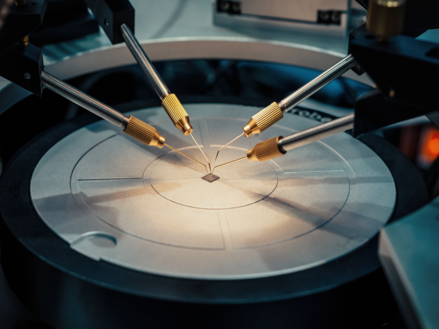
When you couple our experience in Failure Analysis, design verification/validation, and test automation with our tools and expertise to create application specific debug solutions the result is the perfect culmination of engineering disciplines to resolve the most challenging product debug issues. Whether wafer level, bare die, package level, or board level, Watson Analytical is your best option to address all your product debug needs.

Industries
Who We Are