
Laser assisted device alteration (LADA) is an advanced laser injection fault isolation technique utilized when static fault isolation techniques are not successful in isolation a failure mechanism. LADA is effective in localizing the following failure modes and mechanisms:
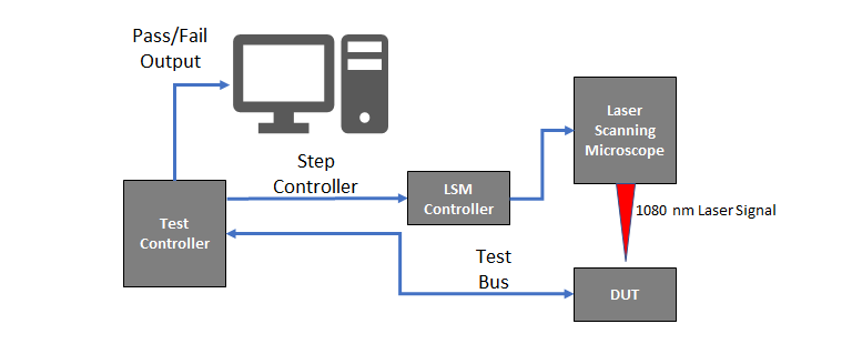
The foundation to a LADA system is a scanning laser microscope (LSM) with the core of the technique and system being the test controller. With the LSM focus on a point, the test controller excutes an automated electrical test on the DUT and analyzes the data collected during testing. If the device operated within specification, a "PASS" output is passed to the imaging sofware on the computer, but if the test controller determines the device is operating outside specificiation, a "FAIL" ouput is passed to the imaging software on the computer. The test controller then steps the LSM to the next pixel where the test controller subsequently performs the electrical test. Throught this iterative process, the test controller steps the LSM over a defined area of the DUT building a mosaic of PASS/FAIL pixels on the imaging computer to highlight the location of a failure mechanism. The image below details the major components of a LADA system.
The semiconductor substrate of the device is thinned and polished to provide the implant, diffusion, and junction regions direct exposure to the laser signal (Figure 2). A laser signal with a wavelength of 1080nm is used to generate electron-hole pairs in the PN junctions to alter the electrical behavior of a device. In a PMOS device, the majority of electron-hole pairs are generated at the n-well to p-substrate interface effectively reducing the n-well bias voltage and a lower threshhold voltage is realized for the PMOS device. Conversely in an NMOS device, the electron-hole pairs are generated at the PN junctions of the source/drain resulting in leakage current to the p-substrate resulting in an increase of the effective threshold volage.
Applying physics of LADA to simple logic inverter circuit, Figure 3 demonstrates the in circuit effect of LADA. The blue solid blue waveform at the input of the inverter represents input signal/data. The dashed blue waveform out the output represents the output signal/data seen at the output under normal conditions. The yellow waveform illustrates how LADA alterates the signal/data seen at the output of the inverter. In short, the inverter "turns on" sooner and "turns off" later.
 Figure 3: This image shows a signal applied to the input of a logic inverter circuit. The dashed blue waveform shows the signal at the output under normal conditions, while the yellow waveform illustates the effect of LADA on the waveform at the output.
Coupling our undersanding of the effect LADA has on active circuitry under transient conditions with a comprehensive set of electrical characterization data, such as a shmoo plot (Figure 4), parameters such as bias and test conditions may be optimized to ensure success. In the example show in FIgure 4, the shmoo plot show the clock and VDD conditions under which the DUT passes and fails. For this example, we imply the device is biased and tested under the highlight failiing condition. When subsequently running LADA, the shift is timing alters the electrical behavior of the DUT causing it to pass electrical testing. The sensitive node which caused the DUT to behave normally would then be plotter on a reference image of the DUT.
- Timing margin
- Race conditions
- Hot carrier injection
- Process Variation
- Vt shifts
- Leff shifts
- Weff shifts
- Diffussion resistance
- Transconductance
- Sub-threshhold leakage
- Ultra thin oxide soft breakdown
- Resistive interconnects
The foundation to a LADA system is a scanning laser microscope (LSM) with the core of the technique and system being the test controller. With the LSM focus on a point, the test controller excutes an automated electrical test on the DUT and analyzes the data collected during testing. If the device operated within specification, a "PASS" output is passed to the imaging sofware on the computer, but if the test controller determines the device is operating outside specificiation, a "FAIL" ouput is passed to the imaging software on the computer. The test controller then steps the LSM to the next pixel where the test controller subsequently performs the electrical test. Throught this iterative process, the test controller steps the LSM over a defined area of the DUT building a mosaic of PASS/FAIL pixels on the imaging computer to highlight the location of a failure mechanism. The image below details the major components of a LADA system.
Figure 1: This image shows the basic configuration of a typical LSM system configured
for laser assisted device alteration (LADA).
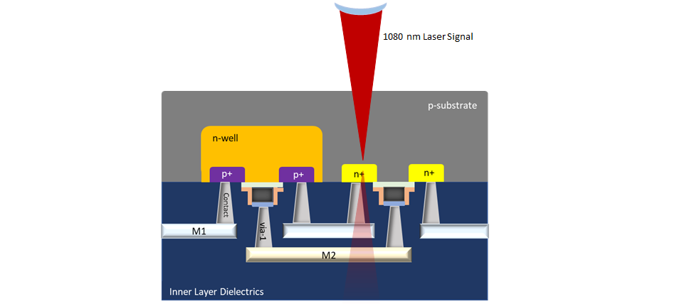
The semiconductor substrate of the device is thinned and polished to provide the implant, diffusion, and junction regions direct exposure to the laser signal (Figure 2). A laser signal with a wavelength of 1080nm is used to generate electron-hole pairs in the PN junctions to alter the electrical behavior of a device. In a PMOS device, the majority of electron-hole pairs are generated at the n-well to p-substrate interface effectively reducing the n-well bias voltage and a lower threshhold voltage is realized for the PMOS device. Conversely in an NMOS device, the electron-hole pairs are generated at the PN junctions of the source/drain resulting in leakage current to the p-substrate resulting in an increase of the effective threshold volage.
Figure 2: This image illustrates the laser signal interacting with
the active circuitry of the device substrate.
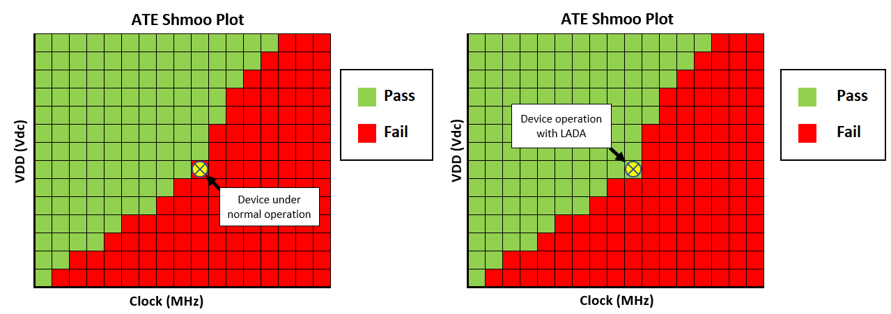
Coupling our undersanding of the effect LADA has on active circuitry under transient conditions with a comprehensive set of electrical characterization data, such as a shmoo plot (Figure 4), parameters such as bias and test conditions may be optimized to ensure success. In the example show in FIgure 4, the shmoo plot show the clock and VDD conditions under which the DUT passes and fails. For this example, we imply the device is biased and tested under the highlight failiing condition. When subsequently running LADA, the shift is timing alters the electrical behavior of the DUT causing it to pass electrical testing. The sensitive node which caused the DUT to behave normally would then be plotter on a reference image of the DUT.
Figure 4: Example of a shmoo characterization of a device. The shmoo plot on the left points out clock and VDD conditions under which the DUT fails to pass test limits. The shmoo plot on the right shows the electrical behavior of the DUT altered by LADA passing the test limits.