
Soft defect localization (SDL) is an advanced fault isolation technique used to isolate functional failures induced by ohmic related defects, damage, or degradation. SDL would be applied when a failure mechanism cannot be isolated by other static fault isolation techniques such as photon emission microscopy, thermal hotspot, or externally induced voltage alteration (XIVA).
SDL is effective in isolating thermal sensitive latent defects or damage in the following conditions:
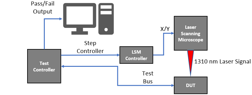
Figure 1 shows a basic block diagram of an SDL system. The core of the SDL technique is the block labeled “Test Controller”. The test controller is a poly-functional component in this system. This block controls the scan and stepping of the laser scanning microscope, performs electrical testing of the DUT, and provides a pass/fail test result to the system computer/software. In operation, the laser signal starts out at an initial position. The test controller performs the electrical test on the DUT. If the DUT passes electrical testing, the test controller sends a pass code to the computer to be plotted as a single pixel on the SDL image. Following electrical testing, the test controller sends a step command to the LSM and moves the laser signal to the next pixel position. The DUT test is executed, the pass/fail result is sent to the computer. The laser signal is scanned/stepped in an iterative process until the SDL image has been rendered over the defined scan area. A failed test may be plotted as a red colored pixel, and a passed test may be plotted as a green pixel resulting in an SDL image which highlights the locations of failure mechanisms.
The core physics behind SDL relys on the thermal coeficient of material the laser signal is interacting with. Equation (1) describes the resistive behavior of a static material for a given thermal coefficent alpha. Formula (2) describes the resistive behavior of a field effect transistor (FET) for a given thermal coefficient alpha. At the basic level, these equations predict that, with thermal stimulation, the resistance of a material may be altered with the application of a heat source resulting in a measureable and observable change of in circuit current.
SDL may be performed from the top of a device, as shown in Figure 2, or through the backside of the substrate. A laser signal of wavelength 1310 nm is used to inject the thermal stimulus to a focused point in the device. As the laser signal is scanned across the device the resistance of the material changes shifting the electrical behavior of the device. Defects and damage commonly cover a small area and/or volume, relative to normal circuit features; this results in large variations in device behavior when thermal stimulation is imparted on damage/defects.
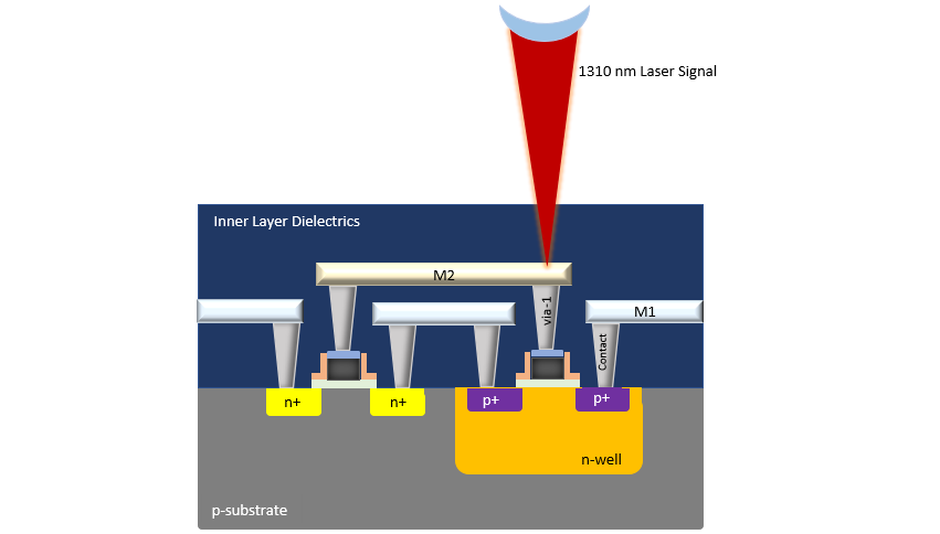
Figure 3 shows a logic inverter circuit with a good signal (solid blue line) at the input, but significant degradation can be seen in the signal (blue dashed line) at the output. This type of circuit behavior is commonly caused by malformed vias/contacts resulting in a high resistance connection and preciptiates out as a functional timing failure. When running SDL the thermal stimulus of the laser signal causes the contact/via to physically expand increasing the contact area, reducing contact resistance, and improving the output signal as illustrated by the solid yellow line in Figure 3. This causes the device operation to shift from a failing operation as shown in the left shmoo plot in Figure 4 to a pass operation as shown in the right shmoo plot in the same figure.

Figure 3: The solid line blue waveform represents the signal at the input of the inverter. The dashed blue waveform represents the signal at the output of the inverter under typical operatiing conditions. The yellow waveform illustrates the effect SDL may have on the operation of the circuit.
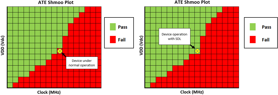
Figure 4: The images above are fabricated shmoo plots used to illustrate the effects of SDL on a DUT. The shmoo characterization plot on the left shows the device behavior under typical operating conditions over clock and VDD; the comment box points to an abitrary failure point. The comment box in the shmoo plot on the right points out the same point passing with SDL.
SDL is effective in isolating thermal sensitive latent defects or damage in the following conditions:
- Scan chain
- Register read
- Register write
- Race condition
- Schmoo
- Generic Functional
- Open via/contact
- Stringers
- Gate Oxide Shorts
Figure 1 shows a basic block diagram of an SDL system. The core of the SDL technique is the block labeled “Test Controller”. The test controller is a poly-functional component in this system. This block controls the scan and stepping of the laser scanning microscope, performs electrical testing of the DUT, and provides a pass/fail test result to the system computer/software. In operation, the laser signal starts out at an initial position. The test controller performs the electrical test on the DUT. If the DUT passes electrical testing, the test controller sends a pass code to the computer to be plotted as a single pixel on the SDL image. Following electrical testing, the test controller sends a step command to the LSM and moves the laser signal to the next pixel position. The DUT test is executed, the pass/fail result is sent to the computer. The laser signal is scanned/stepped in an iterative process until the SDL image has been rendered over the defined scan area. A failed test may be plotted as a red colored pixel, and a passed test may be plotted as a green pixel resulting in an SDL image which highlights the locations of failure mechanisms.
Figure 1: Basic block diagram of the SDL system.
The core physics behind SDL relys on the thermal coeficient of material the laser signal is interacting with. Equation (1) describes the resistive behavior of a static material for a given thermal coefficent alpha. Formula (2) describes the resistive behavior of a field effect transistor (FET) for a given thermal coefficient alpha. At the basic level, these equations predict that, with thermal stimulation, the resistance of a material may be altered with the application of a heat source resulting in a measureable and observable change of in circuit current.
SDL may be performed from the top of a device, as shown in Figure 2, or through the backside of the substrate. A laser signal of wavelength 1310 nm is used to inject the thermal stimulus to a focused point in the device. As the laser signal is scanned across the device the resistance of the material changes shifting the electrical behavior of the device. Defects and damage commonly cover a small area and/or volume, relative to normal circuit features; this results in large variations in device behavior when thermal stimulation is imparted on damage/defects.
Figure 2: Cross-section image of an inverter circuit interacting
with a thermal stimulus from a laser injected signal.
with a thermal stimulus from a laser injected signal.
Figure 3 shows a logic inverter circuit with a good signal (solid blue line) at the input, but significant degradation can be seen in the signal (blue dashed line) at the output. This type of circuit behavior is commonly caused by malformed vias/contacts resulting in a high resistance connection and preciptiates out as a functional timing failure. When running SDL the thermal stimulus of the laser signal causes the contact/via to physically expand increasing the contact area, reducing contact resistance, and improving the output signal as illustrated by the solid yellow line in Figure 3. This causes the device operation to shift from a failing operation as shown in the left shmoo plot in Figure 4 to a pass operation as shown in the right shmoo plot in the same figure.
Figure 3: The solid line blue waveform represents the signal at the input of the inverter. The dashed blue waveform represents the signal at the output of the inverter under typical operatiing conditions. The yellow waveform illustrates the effect SDL may have on the operation of the circuit.
Figure 4: The images above are fabricated shmoo plots used to illustrate the effects of SDL on a DUT. The shmoo characterization plot on the left shows the device behavior under typical operating conditions over clock and VDD; the comment box points to an abitrary failure point. The comment box in the shmoo plot on the right points out the same point passing with SDL.