
As integrated circuit technologies shrink and metal layers increase the density of the integrated circuit layouts negatively impacting efficacy of typical fault isolation techniques. Photons generated by electron whole-pair recombination are increasingly less like to propagate to the passivation layer and ultimately escaping the die to be detected with a techniques like Photon Emission microscopy (PEM / EMMI). Conversely, propagating an external stimulus through the passivation and metal layers to excite a failure mechanism in the substrate or lower metal layers becomes more difficult as circuit density increases. This issue is resolved with area defined backside preparation processing technology.
Area defined backside preparation is a process by which the backside or bottom of the die is exposed and polished to a mirror finish. At the start of this process, the X-axis and Y-axis scan parameters are setup to define a specific area to be milled and polished. The plastic covering the die is then removed with a diamond bit to expose the package paddle, if present. The paddle is subsequently removed from the package with an endmill bit to expose the die attach. A diamond bit is loaded back on the system to remove the die attach epoxy and thin the die to the desired die thickness. The die is then polished with a combination of diamond suspensions, slurries, and colloidals.
This process may be used to augment or improve the performance of multiple semiconductor fault isolation techniques. When utilizing PEM/EMMI, photons generated in the semiconductor substrate are detected by a detector. Device metallization blocks photons when PEM/EMMI is performed from the topside of the device. With backside prep, PEM/EMMI is performed through the semiconductor substrate with a direct unobstructed exposure to the source of the photon emissions, significantly advancing the effectiveness of this analysis technique.
When utilizing laser based fault isolation techniques it is critical the laser stimulus reach the site of the failure mechanism for successful detection. If the analysist is running optical beam induced current (OBIC), it is absolutely imperative the laser signal have an unobstructed path to semiconductor junctions. With high count metal layers and high density circuitry the challenge is tangible. Area defined backside preparation eliminates obstructions created from high density and high metal count fabricated devices optimizing the probability for success for failure mechanisms at lower metal levels and semiconductor junctions.
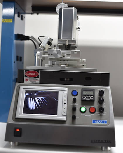
The ASAP-1 Analog Select Area Preparation System is a multi-application system manufactured by ULTRA_TEC This is an excellent system which we leverage for many of our advanced sample preparation techniques.
Area defined backside preparation is a process by which the backside or bottom of the die is exposed and polished to a mirror finish. At the start of this process, the X-axis and Y-axis scan parameters are setup to define a specific area to be milled and polished. The plastic covering the die is then removed with a diamond bit to expose the package paddle, if present. The paddle is subsequently removed from the package with an endmill bit to expose the die attach. A diamond bit is loaded back on the system to remove the die attach epoxy and thin the die to the desired die thickness. The die is then polished with a combination of diamond suspensions, slurries, and colloidals.
This process may be used to augment or improve the performance of multiple semiconductor fault isolation techniques. When utilizing PEM/EMMI, photons generated in the semiconductor substrate are detected by a detector. Device metallization blocks photons when PEM/EMMI is performed from the topside of the device. With backside prep, PEM/EMMI is performed through the semiconductor substrate with a direct unobstructed exposure to the source of the photon emissions, significantly advancing the effectiveness of this analysis technique.
When utilizing laser based fault isolation techniques it is critical the laser stimulus reach the site of the failure mechanism for successful detection. If the analysist is running optical beam induced current (OBIC), it is absolutely imperative the laser signal have an unobstructed path to semiconductor junctions. With high count metal layers and high density circuitry the challenge is tangible. Area defined backside preparation eliminates obstructions created from high density and high metal count fabricated devices optimizing the probability for success for failure mechanisms at lower metal levels and semiconductor junctions.
The ASAP-1 Analog Select Area Preparation System is a multi-application system manufactured by ULTRA_TEC This is an excellent system which we leverage for many of our advanced sample preparation techniques.