
Photon emission microscopy (PEM) is a fault isolation technique which, like many analytical techniques, is recognized by various names and acronyms. The moniker photon emission microscopy is synonymous photoemission microscopy (PM), emission microscopy (EMMI), and light emission microscopy (LEM). The PEM system consists of a photon detector, light tight enclosure, and the device under test (DUT).
This fault isolation technique is effective in detecting failure mechanism related to the following electrical behaviors:
Fundamentally PEM is able to isolate failure mechanisms by detect photon emission generated by electron-hole pair recombination under two transition conditions, interband recombination and intraband recombination.
During interband recombination, a free electron in the conduction band fills a lower energy state in the valence band. In order for the electron to fill the lower energy state it must “give up” energy and does so in the form of a photon. There are two modes under which interband recombination emissions are generated. Under the first mode, the electron transitions from the conduction band directly to the valance band with a transition energy of 3.3 eV releasing a photon with a wavelength of approximately 376nm; the is representative of a normal working device. Under the second mode, the electron undergoes an indirect transition when the electron transitions to a band energy other than the maximum. This condition is primarily caused due to damage or defects in the DUT generating a photon at 1.1eV with a wavelength of approximately 1127nm. The bimodal nature and generous separation of photon wavelengths permits the normal photon emission to be filtered out while optimizing the detector to detect damage and/or defects in devices.
Intraband recombination is the energy band(s) for light hole flow and heavy hole flow in the semiconductor materials. Under dynamic conditions, such as clocking, switching, signal processing, transition may occur between these two energy bands (intraband recombination) where hole current is present. The intraband recombination releases low energy photons (<1.0 eV) with wavelengths longer than 1240 nm.
There are a variety of effective detector options available when considering a PEM system. The most common detectors are charge couple devices (CCDs) and indium gallium arsnide (InGaAs); mercury cadmium telluride (MerCad Tellride, MCT, MerCat) has been used in the past but is less common in more recent PEM solutions.
The broadest range of options come from CCD based technologies, and there are a few key specifications we consider when choosing a CCD detector. Back-illuminated CCD arrays detect the signal through the substrate eliminating interference from metal routing over the array pixels improving maximum array sensitivity. Readout noise is the variation of electrons measured from the array due to random fluctuations of the read out amplifier. As readout noise increases, DUT failure mechanisms exhibiting low leakage currents may be lost in read out noise, so it’s desirable to select a detect with the lowest readout noise available. Dark current noise is generated by thermal energy in the substrate lattice. Dark current noise will continue to fill the well over the period of the exposure, therefore the detector would never be capable of detecting a failure mechanism exhibiting a leakage low than the dark current noise of the CCD. To minimize dark current, the CCD is cooled thermo-electrically (peltier device) or liquid nitrogen (LN2). Well depth is the maximum number of electrons the well may store of the course of the photo emission exposure. The maximum exposure time capability scales with well depth; deep wells are desirable for running extended PEM exposures for extreme low leakage failure mechanisms. Optical filtering is used to tune the CCD to detect specific wavelengths in order to optimize detector sensitivity to the desired events. Key advantages of the CCD detector are low noise, moderate sensitivity, and long exposure time capability making it our first choice for PEM detectors. Learn more about the fundamentals of CCDs here: CCD_Fundamentals
The InGaAs detector is rated by the same specifications as the CCD detector. While the InGaAs Detector is typically more sensitive, the detector is severely limited due to the level of dark current. Learn more about the InGaAs detector here: InGaAs_Basics
Lastly the MCT detector was a popular choice for detectors in the early 2000’s for its sensitivity in the short wave infrared (SWIR) spectrum. With the application of the appropriate filters, the detector could be utilized for both PEM and thermal hot spot applications. A major contributing factor which lead to MCT detectors falling out of favor was it’s tendency to deteriorate rapidly, relative to the comparable technologies above.
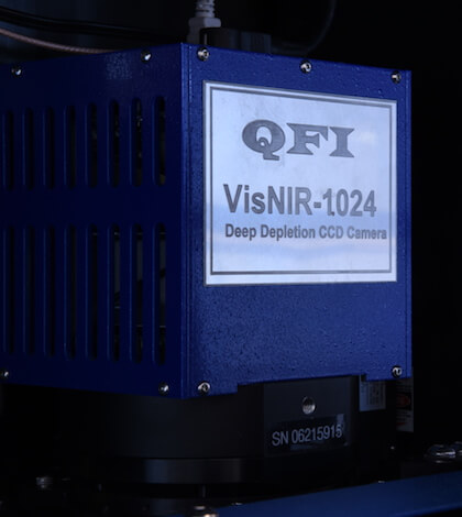
Following a rigorous equipment evaluation of PEM systems across the industry, we selected the Quantum Focus Multi-sensor System equipped with the VisNIR-1024 detector for its excellent performance. While under evaluation this system successfully detected 70nA of leakage through a standardized diode circuit. For more information on this system please visit QFI’s website for this system at: emmi_Photoemission_Microscopy
This fault isolation technique is effective in detecting failure mechanism related to the following electrical behaviors:
- Forward Biased Junctions
- Avalanche Junctions (Reverse Bias)
- Junction Damage/Defect Leakage
- Junction Breakdown Leakage
- Oxide Overstress Breakdown
- Oxide Damage/Defect Breakdown
- Excessive Oxide Leakage
- Hot Electrons
- Latch-up
- Saturated Bipolar Transistors
- Saturated Field Effect Devices
- Saturate Metal Oxide Semiconductor (MOS) Devices
- ESD Related Damage
- Crystal Pipe Related Defects
- Crystal Dislocation Related Defects
- Contact Spiking
- Polysilicon Filaments
- Substrate Damage
Fundamentally PEM is able to isolate failure mechanisms by detect photon emission generated by electron-hole pair recombination under two transition conditions, interband recombination and intraband recombination.
During interband recombination, a free electron in the conduction band fills a lower energy state in the valence band. In order for the electron to fill the lower energy state it must “give up” energy and does so in the form of a photon. There are two modes under which interband recombination emissions are generated. Under the first mode, the electron transitions from the conduction band directly to the valance band with a transition energy of 3.3 eV releasing a photon with a wavelength of approximately 376nm; the is representative of a normal working device. Under the second mode, the electron undergoes an indirect transition when the electron transitions to a band energy other than the maximum. This condition is primarily caused due to damage or defects in the DUT generating a photon at 1.1eV with a wavelength of approximately 1127nm. The bimodal nature and generous separation of photon wavelengths permits the normal photon emission to be filtered out while optimizing the detector to detect damage and/or defects in devices.
Intraband recombination is the energy band(s) for light hole flow and heavy hole flow in the semiconductor materials. Under dynamic conditions, such as clocking, switching, signal processing, transition may occur between these two energy bands (intraband recombination) where hole current is present. The intraband recombination releases low energy photons (<1.0 eV) with wavelengths longer than 1240 nm.
There are a variety of effective detector options available when considering a PEM system. The most common detectors are charge couple devices (CCDs) and indium gallium arsnide (InGaAs); mercury cadmium telluride (MerCad Tellride, MCT, MerCat) has been used in the past but is less common in more recent PEM solutions.
The broadest range of options come from CCD based technologies, and there are a few key specifications we consider when choosing a CCD detector. Back-illuminated CCD arrays detect the signal through the substrate eliminating interference from metal routing over the array pixels improving maximum array sensitivity. Readout noise is the variation of electrons measured from the array due to random fluctuations of the read out amplifier. As readout noise increases, DUT failure mechanisms exhibiting low leakage currents may be lost in read out noise, so it’s desirable to select a detect with the lowest readout noise available. Dark current noise is generated by thermal energy in the substrate lattice. Dark current noise will continue to fill the well over the period of the exposure, therefore the detector would never be capable of detecting a failure mechanism exhibiting a leakage low than the dark current noise of the CCD. To minimize dark current, the CCD is cooled thermo-electrically (peltier device) or liquid nitrogen (LN2). Well depth is the maximum number of electrons the well may store of the course of the photo emission exposure. The maximum exposure time capability scales with well depth; deep wells are desirable for running extended PEM exposures for extreme low leakage failure mechanisms. Optical filtering is used to tune the CCD to detect specific wavelengths in order to optimize detector sensitivity to the desired events. Key advantages of the CCD detector are low noise, moderate sensitivity, and long exposure time capability making it our first choice for PEM detectors. Learn more about the fundamentals of CCDs here: CCD_Fundamentals
The InGaAs detector is rated by the same specifications as the CCD detector. While the InGaAs Detector is typically more sensitive, the detector is severely limited due to the level of dark current. Learn more about the InGaAs detector here: InGaAs_Basics
Lastly the MCT detector was a popular choice for detectors in the early 2000’s for its sensitivity in the short wave infrared (SWIR) spectrum. With the application of the appropriate filters, the detector could be utilized for both PEM and thermal hot spot applications. A major contributing factor which lead to MCT detectors falling out of favor was it’s tendency to deteriorate rapidly, relative to the comparable technologies above.
Following a rigorous equipment evaluation of PEM systems across the industry, we selected the Quantum Focus Multi-sensor System equipped with the VisNIR-1024 detector for its excellent performance. While under evaluation this system successfully detected 70nA of leakage through a standardized diode circuit. For more information on this system please visit QFI’s website for this system at: emmi_Photoemission_Microscopy