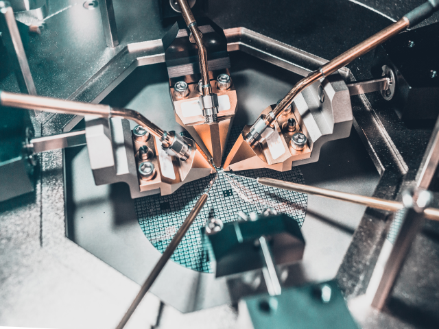
Semiconductor characterization is foundationally vitalto every successfully launch product released to and adopted by the open market.
Fill Out A Quick Form and Get A Free Quote!
Depending on where your team’s role is in the product development cycle,semiconductor characterization has many names: device characterization, intellectual property (IP) block design validation, IP block verification, design validation, design verification, and product characterization, to name a few.
Naturally as engineers, we want to collect as much data as possible during these design characterization phases, and it is common for the list of desired data to exceed the resource bandwidth of the equipment and staff available at peak development cycles.
Through these periods of development Watson Analytical offers a wide array of options to support your product characterization needs at both the wafer and package level. We can work with characterization plan and test solutions defined by the customer, and we are also able to propose and implement a test solution for product characterization.
Characterization Applications
- Digital Characterization
- Analog Characterization
- RF/Microwave Characterization
- Device characterization
- Intellectual Property (IP) Block Characterization
- Design Validation
- Design Verification
- Product Validation
- Product Characterization
Measurement Techniques Examples
- Rise/Fall Time
- Settling Time
- Slew Rate
- Phase Noise
- Noise Figure
- SNR
- CMRR
- Compression
- IIP3
- IOP3
- Harmonics
- Intermodulation Distortion (IMD)
- RF breakdown
- Scatter Parameters (S-parameters)
- Insertion loss
- Isolation
- Gain
- Parametric
- I/V
- I DS /V GS
- I gs
- A V
- Alpha
- Beta
- Custom customer defined

Industries
Who We Are